
Ever wondered how a tiny switch inside your computer can set off a whole chain of actions? Digital design and computer architecture are like the backbone of all the technology we use every day.
Imagine little logic gates working together like a well-practiced band. They join forces, triggering a sequence of operations, much like the parts of a finely tuned machine coming together on stage.
In this article, we’ll show you how clever design choices boost performance while keeping energy use low. It’s all about that innovative edge which makes our everyday devices run smoothly, almost as if by magic.
Foundational Principles of Digital Design and Computer Architecture
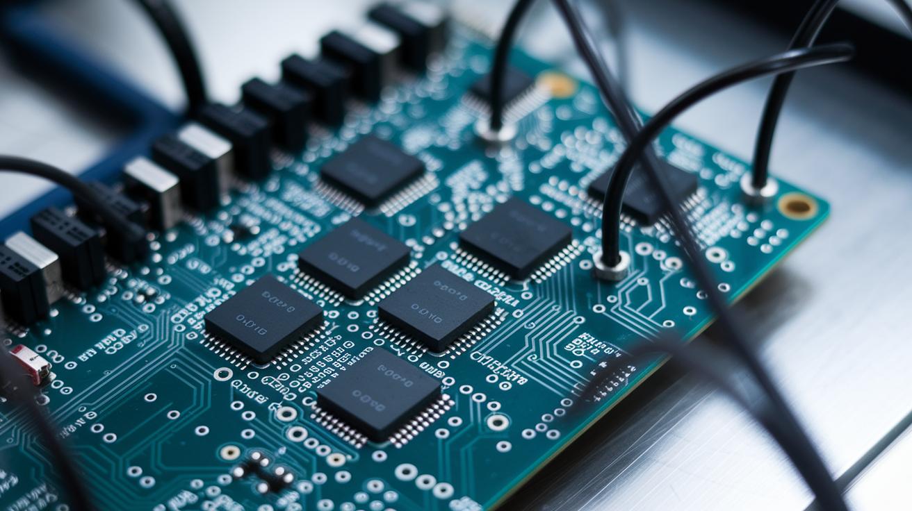
Digital design kicks off with a clear view that covers everything from tiny gates to full-fledged systems. At its most basic, simple logic gates like AND, OR, and NOT work together as the building blocks. These little elements team up to form modules that handle more complex jobs. Imagine a tiny spark lighting up a circuit – that’s how one gate can set off a chain reaction, letting all the parts work in harmony.
Computer architecture builds on this base using layers that stack up like a well-crafted sandwich. First, the instruction set architecture tells the system what to do, much like following a simple recipe. Then, microarchitecture groups together essential parts like registers, arithmetic units, and buses into smart teams that process information. Finally, system integration brings every piece together, similar to assembling parts into a finely tuned instrument. It’s where raw potential really turns into real, tangible power.
Early design choices have a big impact on overall performance and energy use. How you arrange circuits and set up data paths can make a processor run faster and sip power instead of guzzling it. As systems get more complex and our needs grow, these smart decisions help boost speed and reliability while keeping energy use under control. In truth, every layer of design plays a vital role in creating strong, efficient computing platforms.
Logic Circuit Design: Combinational and Sequential Analysis in Architecture
When you dive into digital systems, logic circuit design becomes the heartbeat of the tech world. It breaks down into two types: combinational logic and sequential logic. Combinational logic gives outputs based solely on what you feed it right now, kind of like flipping a light switch that changes state instantly. Sequential logic, on the other hand, remembers its past moves and mixes that with the current inputs to decide what comes next, imagine a counter that keeps track of every flip.
Take a look at these simple building blocks:
- AND: Lights up only when every input is on, think of it as pressing two buttons that make the light shine brightly.
- OR: Gives a high signal when at least one input is active, just like any button press creates a little spark.
- NOT: Flips the input, turning a high into a low or vice versa, it's like switching the scene completely.
- NAND: Outputs low only when all inputs are on, serving as a key part in many designs, even when everything seems set, one twist can change the whole vibe.
| Logic Type | Characteristic | Use Case |
|---|---|---|
| Combinational | Outputs depend only on current inputs | Arithmetic circuits, data routing |
| Sequential | Outputs depend on current inputs and stored state | Memory elements, state machines |
Timing and memory play a big part when you mix these designs. Sequential circuits, for instance, need a good clocking system to catch and hold onto their states over time. This lets them handle everything from simple counters to the more complex memory banks. It’s like enjoying a concert; you need to catch every beat and moment to feel the full energy. This blend of remembering the past while handling new inputs is what fuels today’s dynamic digital adventures.
Microarchitecture Innovations: Data Paths, Control Units, and Pipelining

Datapath parts like the arithmetic logic unit (ALU), registers, and buses form the heart of any processor. The ALU is like the engine that does all the math and logic, while registers quickly hold temporary data. Buses are the pathways that carry all this information around, much like busy city streets where data zips from one place to another.
The control unit is the director of this show, telling everything when and how to work. With hardwired control, fixed circuits send signals on a set schedule, think of it as a strict daily routine. In contrast, microprogrammed control uses a list of small instructions, which gives the system some wiggle room to adjust on the fly, kind of like a flexible switch that adapts to what’s needed.
Imagine a five-step assembly line for handling instructions. It starts with the fetch stage, where an instruction is picked up. Next comes the decode stage, which figures out what the instruction means. Then, the execute stage does the actual work, followed by the memory stage that handles data storage and retrieval. Finally, the write-back stage updates the registers with the new results. Here’s a cool fact: in many modern chips, the decode stage can process hundreds of instructions every second, turning simple commands into powerful actions.
There are trade-offs when it comes to pipeline depth and clock frequency. A longer pipeline can speed things up by processing more steps at once, but if one stage dawdles, it might slow everything down. A shorter pipeline is easier to manage but might not reach the same speeds. It’s a bit like tuning a racecar engine, more power is great until you risk losing that perfect balance between speed and control.
Hardware Description Languages: Verilog and VHDL in Digital Architecture

Imagine a tiny digital calculator coming to life on your screen. The Verilog example below shows a simple 4-bit adder that takes two small numbers, adds them together, and even tells you if there’s a carryover. It keeps things clear with easy port definitions and a crisp assign statement that handles all the math. Check it out:
module four_bit_adder(
  input [3:0] a,
  input [3:0] b,
  output [3:0] sum,
  output carry
);
  assign {carry, sum} = a + b;
endmodule
This snippet sets up two 4-bit inputs and produces both a 4-bit sum and a carry flag. Imagine the thrill of seeing basic math happen so smoothly, it’s like peeling back the curtain on how early digital calculators performed those quick operations.
Now, let’s switch gears to VHDL. Here, the same 4-bit adder takes shape using an entity and an architecture block. Think of it as building a blueprint where every signal and step is clearly laid out. The VHDL code uses explicit signal declaration and a process block to handle the addition operation, which makes it really easy to follow along. Here’s the guide:
entity four_bit_adder is
  Port (
    a     : in  std_logic_vector(3 downto 0);
    b     : in  std_logic_vector(3 downto 0);
    sum   : out std_logic_vector(3 downto 0);
    carry : out std_logic
  );
end four_bit_adder;

architecture Behavioral of four_bit_adder is
begin
  process(a, b)
    variable temp: unsigned(4 downto 0);
  begin
    temp := unsigned(a) + unsigned(b);
    sum   <= std_logic_vector(temp(3 downto 0));
    carry <= temp(4);
  end process;
end Behavioral;
This VHDL version highlights the step-by-step process behind the scenes. It details how signals work together and how each small piece of data moves through the system, almost like watching a well-rehearsed dance. And while creating testbenches to try out these codes, you get a hands-on look at how inputs change into real results.
Both approaches have their own charm and style, showing us that digital design can be just as creative and engaging as any live performance.
System-Level Integration: SoC Strategies and FPGA Prototyping Workflows

FPGA Prototyping Workflow
Working on an FPGA prototype is like putting together a cool puzzle. You start by loading your design files into an FPGA toolchain, where your hardware description code is transformed into digital logic. Imagine it like loading a puzzle into a box; your code then becomes a netlist that clearly shows how all the pieces connect. Next, the process of placing and routing figures out exactly where each part goes on the chip. It's a bit like mapping out your puzzle so that every piece fits perfectly. Finally, the bitstream is loaded onto a development board for testing, and when the board runs your design, you get a real sense of satisfaction as you see it all come to life.
SoC Integration Strategies
Integrating an SoC brings together different parts like CPU cores, memory controllers, and custom IP into one complete chip. The journey starts with careful planning, kind of like organizing distinct pieces on a board so that none of them overcrowd each other. After you set the layout, you check each signal path to make sure everything meets the performance goals, ensuring the chip runs smoothly without any delays. For example, if the memory controller keeps in step with the CPU core, you know the design is solid. This thoughtful mix of planning and testing creates a robust system that can handle high-demand tasks reliably.
Performance Optimization Techniques in Digital Design and Computer Architecture

Maximizing performance means boosting the flow of work and reducing delays. It all revolves around key metrics like instructions per cycle (IPC), latency, and throughput. Think of IPC as counting high-fives during a live show, each cycle brings a burst of energy. Latency is simply the wait between pressing a button and seeing the result, while throughput is about how many tasks get done in a given time, like a busy factory where every second matters.
Hardware conflicts can slow things down. Sometimes parts of the processor clash over the same resource, and that's called a structural hazard. Then, you have data hazards, which happen when an instruction has to wait for another to finish. And don't forget control hazards, which pop up when the path of execution changes unexpectedly, like a sudden detour during a live performance.
| Hazard Type | Resolution Technique |
|---|---|
| Structural | stall |
| Data | forwarding |
| Control | speculation |
Cache hierarchies work kind of like a layered storage system. The smallest and fastest caches are right next to the processor, ready to deliver data in an instant. Then, larger caches hold more information even if they're a bit slower. This balance keeps the processor busy, much like a well-prepped backstage crew always keeping the show on track. In a similar way, basic branch predictor strategies try to guess the next move in a program. When the guess is spot-on, the data flows smoothly; when it’s off, there’s just a tiny pause before everything picks up again.
Verification, Testing, and Emerging Trends in Computer Architecture Design

Engineers often start with simulation-based methods to check how a system might behave before turning a design into hardware. They mimic real-life actions on the computer to see that every part of the design works as it should. And then, using simple math-based proofs, they confirm that each possible logic path does what it’s meant to do.
Next comes the testbench, which is like running a practice round before the real game. Here, developers feed a bunch of different input scenarios into the design, imagine testing every twist and turn of a roller coaster, to catch any hidden glitches. This smart, step-by-step approach saves time and helps avoid expensive fixes later.
Today, chip design is getting a major upgrade thanks to advanced nodes like 7 nm and 5 nm, which make chips smaller, faster, and more efficient. Plus, new hardware-software co-design techniques now bring firmware and circuits closer together, smoothing out how they interact. Modern design tools, known as EDA suites (electronic design automation tools), let engineers quickly refine their work. These tools check timing paths and spot potential issues early, keeping projects on track and in tune with the latest digital demands.
Final Words
in the action, the article walked through the key ideas behind digital design and computer architecture, breaking down core principles, logic circuit analysis, and microarchitecture components.
We explored how hardware description languages and system-level integration bring these concepts to life and shared techniques to boost system performance. The discussion connected theory with hands-on methods, making technical ideas clear and accessible. The excitement in the action carries forward, inviting more discoveries and shared moments of inspiring innovation.
FAQ
Frequently Asked Questions
Q: Where can I find digital design and computer architecture PDFs and which editions are available?
A: The digital design and computer architecture PDFs offer a clear view into processor design, available in multiple editions including the book PDF, 2nd edition, latest edition, and even special RISC-V versions from trusted sources.
Q: How does the digital design and computer architecture RISC-V edition PDF differ from other versions?
A: The digital design and computer architecture RISC-V edition PDF focuses on the RISC-V instruction set, connecting core digital design concepts with practical processor architecture insights.
Q: What makes the digital design and computer architecture book by David Harris and Sarah Harris a valuable resource?
A: The digital design and computer architecture book by David Harris and Sarah Harris is cherished for its straightforward explanations and practical examples that bring digital design concepts and computer architecture layers to life.
Q: Is there a free download option for digital design and computer architecture PDFs?
A: The digital design and computer architecture PDFs can sometimes be found as free downloads on educational websites, though it’s wise to check copyright information and use reputable sources.
